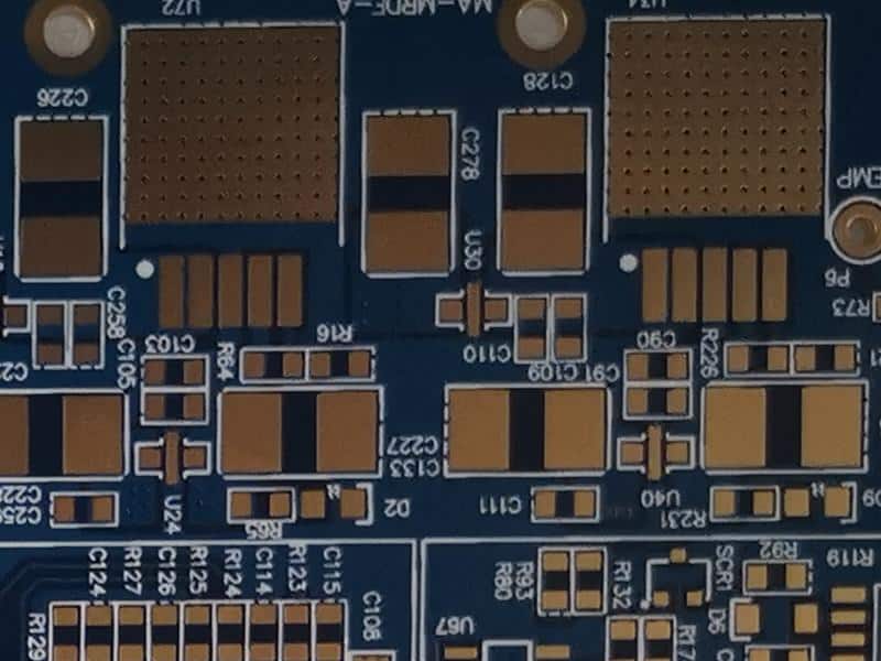
In today's world of advanced technology, electrical circuits and systems are becoming increasingly complex. This requires highly functional and efficient printed circuit boards (PCBs) that can perform multiple functions, support complex applications, and provide the necessary performance and durability.

Multi-layer PCBs are the ideal solution for complex electronic circuitry problems. These high-end circuit boards have multiple layers of conductive material, with insulating layers in between. The layers are then compressed, making them highly efficient and cost-effective.
In this blog, we will take a comprehensive look at 6 layer PCB manufacturing, why you should consider using them, and the benefits they offer.
What is a 6 Layer PCB?
A 6 layer PCB is a printed circuit board with six layers of electrical connectivity. Each layer has a characteristic role, with the top and bottom layers used for the main circuit board, and other layers used for routing, power, and ground planes.
Why Use a 6 Layer PCB?
There are many reasons why you should use a 6 layer PCB for your electronic project. Here are just a few of the benefits it offers:
1. Space-saving: A 6 layer PCB can fit more electrical components, circuits, and systems into a smaller space, making it ideal for small applications.
2. Advanced routing: A 6 layer PCB provides advanced routing options that are necessary for complex systems. The additional layers allow for more routing options, and this enhances circuit performance and reliability.
3. Reduced EMI: Electromagnetic interference (EMI) can negatively affect electrical systems. A 6 layer PCB minimizes EMI, reducing the risk of damage to electronic systems.
4. Enhanced reliability: A 6 layer PCB has improved electrical connectivity and can withstand higher temperatures than other circuit board options.
6 Layer PCB Manufacturing process:
The manufacturing process of a 6 layer PCB involves the following steps:
1. Design and layout: The first step is the design and layout of the PCB. This stage involves creating a schematic diagram and a layout for the PCB.
2. Material selection: The next step is to select the right material for the PCB. The choice of material is crucial, as it determines the performance, durability, and reliability of the circuit board.
3. Layering: In this phase, the individual layers of the PCB are created. This involves affixing a conductive material onto the insulating layers.
4. Drilling: Once the layers have been created and laminated, the PCB is drilled to create holes for components.
5. Plating: At this point, the circuit board is plated with a layer of metal, such as copper, to make the connections between the layers.
6. Etching: This step involves removing any unwanted copper from the circuit board. The areas that are not needed are covered with a masking material, and the exposed copper is etched away.
7. Solder mask and silkscreen: The final step is adding a layer of solder mask and a silkscreen layer. Solder mask provides a protective coating for the circuit board, while the silkscreen is used to label the components.
Conclusion
If you are looking for a comprehensive solution for your complex electronic systems, a 6 layer PCB is an excellent choice. The additional layers provide advanced routing, reduce EMI, and enhance reliability, making them ideal for small applications.
EastwinPCBA is a trusted PCB manufacturer based in China that specializes in high-end PCB fabrication, including 6 layer PCBs. We cater to superior quality 6 layer PCB prototyping needs through our production house in China. If you are looking for cost-efficient and reliable 6 layer PCB fabrication, look no further than EastwinPCBA.